Fundamentals of Microwave and RF Design enables mastery of the essential concepts required to cross the barriers to a successful career in microwave and RF design. Components passive active PWB interconnects do not have the idealized impedances seen at low frequency.

Rf Circuit Design Ch4 2 Lna Pa And Broadband Amplifier
The PowerPoint PPT presentation.
. Techniques are needed that determine the impedance of a component and then how to transform its impedance as necessary. A short summary of this paper. 2 Contents Building blocks in RF system and basic performances Device characteristics in RF application Low noise amplifier design Mixer design Oscillator design.
18 V level for RX and all other modes. This course will enhance your knowledge about Radio Frequency Design which is applied in most of the jobs available in top Wireless and Telecommunication based companies designing. After the talk it will be clear that a circuit with any non negative real.
At the end of this course the student will have depth knowledge of Radio Frequency principles. Typical 2-stage RF PA design V B1 V B2 RF input 50 Ω V POS matching network matching network inductive RF choke allows output to rise above V POS doesnt dissipate power May require additional RF choke here to isolate input from bias circuit Ls and Cs to. The reference book for this course is RF Microelectronics of Behzad Razavi.
The teams main goal while developing the course has been to concentrate more on the. Analysis and design of IQ charge-sharing band-pass-filter for superheterodyne receivers IEEE Transactions on Circuits and Systems I. Market Requirements Architectures Modulation Microwave techniques Standards IC design RF mixed-mode digital Communication Theory TRANSCEIVER Discretes Circuits for Wireless.
Although this concept is mandatory in basic circuit theory curriculums it is repeated for convenience in an appendix. RF circuit design requires impedance transformationsmatching to maximize the transfer of power. Sense small signal amplify with.
This RF module comprises of an RF Transmitter and an RF Receiver. The design of analog and RF circuits in a digital CMOS technology faces many difficulties. Multi-discipline RF design draws upon a multitude of disciplines.
Extensive treatment of scattering parameters that naturally describe power flow and of Smith-chart-based design procedures prepare the student for success. The course covers the topics on how to derive the RF wireless systems specifications. Into RF frequencies or higher the effect of these phase variations becomes a design consideration.
The emphasis is on design at. Do you have PowerPoint slides to share. RF Design is Challenging.
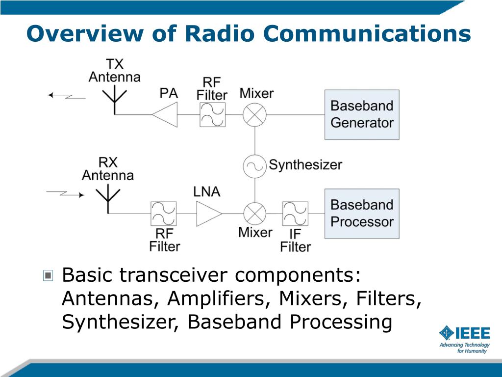
Drive antenna with high power level RX. For the receiver the signal from the antenna is amplified in the radio frequency RF stage. 23 Reflections and Interference.
In RAHRF201 you would get deeper into Radio Frequency Design Theory and Principles. However there are certain components that are highly specific to RF design. The set of available active and passive devices is quite limited the technology is opti-mized for digital design and the devices are characterized and modeled according to.
2 Contents Basic Amplifier Concepts zClass A B C F hHCA zLinearity Aspects zAmplifier Example Enhanced Amplifier Concepts. In this talk we focus our attention on instabilities in the design phase of the circuits where the detection of instabilities is obvious since it is subject to rigorous mathematical analysis. Basics Akira Matsuzawa Tokyo Institute of Technology.
Certain circuit design techniques take advantage of 𝜆 4 and 𝜆 2 effects to optimize or cancel signals which is really a way to minimize the effects of the topic in our next section. Regular Papers 628 2015. Also the method of illustrating and solving network equations by the signal flow graph method is summarized in an appendix.
The output of the RF stage is one input of a mixer. 21 Full PDFs related to this paper. Signals through RF can travel through larger distance.
RF IC design Receiver Transmitter FreqSynth. Directly driven re-entrant RF cavity Outer region. 0V CMOS and GaAs FET switches assures low RX current consumption Simpler control without external LNA No extra signal is needed from MCU to turn off LNA in low power modes RF_P TXRX_SWITCH RF_N CC2420 BALUN TXRX Switch.
Whether a circuit is stable or not in the laboratory. Demand for higher performance lower cost and greater functionality The Big Picture. Full PDF Package Download Full PDF Package.
Download Full PDF Package. Translate circuit model to a cavity model. As with passive components the active components used in RF circuits share many characteristics with active components typically found in lower-frequency analog systems.
Madadi Iman MassoudTohidian and Robert Bogdan Staszewski. This unique Master-level course offered by the Center for Wireless Technology Eindhoven CWTe of the Eindhoven University of Technology The Netherlands provides students with in-depth knowledge and hands-on experience on RF and mmWave circuit design. BASIC LINEAR DESIGN 42 The basic concept of operation is as follows.
A Local Oscillator LO is the other input. Large plate Capacitor Beam Load current I B E Displacement current Wall current a d R L μ o a 2 2 R a C o R2 d o 1 LC c 2R ad R 2a 1 2 Q set by resistance in outer region Q L C R. The output of the mixer is at the Intermediate Frequency IF.
Transmission through RF is better than IR infrared. Trade-offs RF circuits and transceivers must deal with numerous trade-offs. RF Power Amplifier Design Markus Mayer Holger Arthaber Department of Electrical Measurements and Circuit Design Vienna University of Technology June 11 2001.
Large single turn Inductor Central region. The corresponding frequency range varies between 30 kHz 300 GHz. TxRx pair operates at a frequency of 434 MHz.
MOSFET modeling for RF circuit design is the property of its rightful owner. 3 Basic RF circuit block Receiver Transmitter Impedance Matching 1 Low Noise Amp. Power matching is fundamental for designing and understanding many RF circuits.
Up to 10 cash back Finally you will learn about some interesting circuit designs like the RF Power Amplifier PA and the various RF power amplifier architectures and topologies. CC2420EM PA DESIGN Signal from TXRX_Switch pin level shifted and buffered Level in TX. RF Design is Challenging.
Ppt Rf Circuit Design Powerpoint Presentation Free Download Id 5012191

Rf Circuit Design Ch4 2 Lna Pa And Broadband Amplifier
Ppt Rf Circuit Design Powerpoint Presentation Free Download Id 5012191

Rf Circuit Design Ch4 2 Lna Pa And Broadband Amplifier

Rf Circuit Design Ch3 2 Power Waves And Power Gain Expressions

Rf Circuit Design Ch4 2 Lna Pa And Broadband Amplifier
Ppt Design And Modeling Of Rf Circuits Using Design Of Experiments Powerpoint Presentation Id 1587480
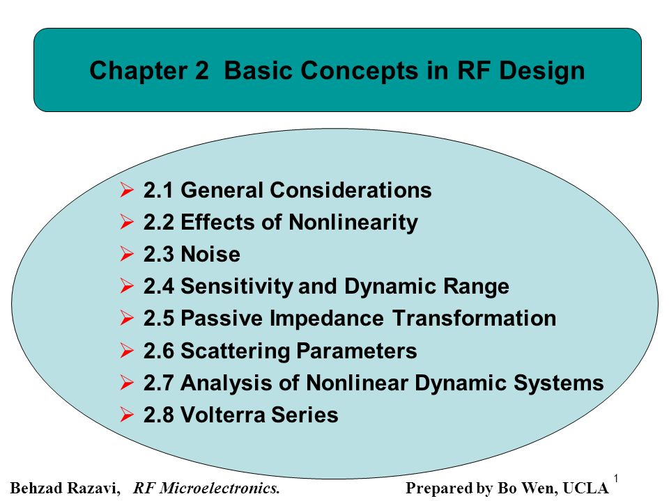
Chapter 2 Basic Concepts In Rf Design Ppt Download
0 comments
Post a Comment